Order Now
- Home
- About Us
-
Services
-
Assignment Writing
-
Academic Writing Services
- HND Assignment Help
- SPSS Assignment Help
- College Assignment Help
- Writing Assignment for University
- Urgent Assignment Help
- Architecture Assignment Help
- Total Assignment Help
- All Assignment Help
- My Assignment Help
- Student Assignment Help
- Instant Assignment Help
- Cheap Assignment Help
- Global Assignment Help
- Write My Assignment
- Do My Assignment
- Solve My Assignment
- Make My Assignment
- Pay for Assignment Help
-
Management
- Management Assignment Help
- Business Management Assignment Help
- Financial Management Assignment Help
- Project Management Assignment Help
- Supply Chain Management Assignment Help
- Operations Management Assignment Help
- Risk Management Assignment Help
- Strategic Management Assignment Help
- Logistics Management Assignment Help
- Global Business Strategy Assignment Help
- Consumer Behavior Assignment Help
- MBA Assignment Help
- Portfolio Management Assignment Help
- Change Management Assignment Help
- Hospitality Management Assignment Help
- Healthcare Management Assignment Help
- Investment Management Assignment Help
- Market Analysis Assignment Help
- Corporate Strategy Assignment Help
- Conflict Management Assignment Help
- Marketing Management Assignment Help
- Strategic Marketing Assignment Help
- CRM Assignment Help
- Marketing Research Assignment Help
- Human Resource Assignment Help
- Business Assignment Help
- Business Development Assignment Help
- Business Statistics Assignment Help
- Business Ethics Assignment Help
- 4p of Marketing Assignment Help
- Pricing Strategy Assignment Help
- Nursing
-
Finance
- Finance Assignment Help
- Do My Finance Assignment For Me
- Financial Accounting Assignment Help
- Behavioral Finance Assignment Help
- Finance Planning Assignment Help
- Personal Finance Assignment Help
- Financial Services Assignment Help
- Forex Assignment Help
- Financial Statement Analysis Assignment Help
- Capital Budgeting Assignment Help
- Financial Reporting Assignment Help
- International Finance Assignment Help
- Business Finance Assignment Help
- Corporate Finance Assignment Help
-
Accounting
- Accounting Assignment Help
- Managerial Accounting Assignment Help
- Taxation Accounting Assignment Help
- Perdisco Assignment Help
- Solve My Accounting Paper
- Business Accounting Assignment Help
- Cost Accounting Assignment Help
- Taxation Assignment Help
- Activity Based Accounting Assignment Help
- Tax Accounting Assignment Help
- Financial Accounting Theory Assignment Help
-
Computer Science and IT
- Operating System Assignment Help
- Data mining Assignment Help
- Robotics Assignment Help
- Computer Network Assignment Help
- Database Assignment Help
- IT Management Assignment Help
- Network Topology Assignment Help
- Data Structure Assignment Help
- Business Intelligence Assignment Help
- Data Flow Diagram Assignment Help
- UML Diagram Assignment Help
- R Studio Assignment Help
-
Law
- Law Assignment Help
- Business Law Assignment Help
- Contract Law Assignment Help
- Tort Law Assignment Help
- Social Media Law Assignment Help
- Criminal Law Assignment Help
- Employment Law Assignment Help
- Taxation Law Assignment Help
- Commercial Law Assignment Help
- Constitutional Law Assignment Help
- Corporate Governance Law Assignment Help
- Environmental Law Assignment Help
- Criminology Assignment Help
- Company Law Assignment Help
- Human Rights Law Assignment Help
- Evidence Law Assignment Help
- Administrative Law Assignment Help
- Enterprise Law Assignment Help
- Migration Law Assignment Help
- Communication Law Assignment Help
- Law and Ethics Assignment Help
- Consumer Law Assignment Help
- Science
- Biology
- Engineering
-
Humanities
- Humanities Assignment Help
- Sociology Assignment Help
- Philosophy Assignment Help
- English Assignment Help
- Geography Assignment Help
- Agroecology Assignment Help
- Psychology Assignment Help
- Social Science Assignment Help
- Public Relations Assignment Help
- Political Science Assignment Help
- Mass Communication Assignment Help
- History Assignment Help
- Cookery Assignment Help
- Auditing
- Mathematics
-
Economics
- Economics Assignment Help
- Managerial Economics Assignment Help
- Econometrics Assignment Help
- Microeconomics Assignment Help
- Business Economics Assignment Help
- Marketing Plan Assignment Help
- Demand Supply Assignment Help
- Comparative Analysis Assignment Help
- Health Economics Assignment Help
- Macroeconomics Assignment Help
- Political Economics Assignment Help
- International Economics Assignments Help
-
Academic Writing Services
-
Essay Writing
- Essay Help
- Essay Writing Help
- Essay Help Online
- Online Custom Essay Help
- Descriptive Essay Help
- Help With MBA Essays
- Essay Writing Service
- Essay Writer For Australia
- Essay Outline Help
- illustration Essay Help
- Response Essay Writing Help
- Professional Essay Writers
- Custom Essay Help
- English Essay Writing Help
- Essay Homework Help
- Literature Essay Help
- Scholarship Essay Help
- Research Essay Help
- History Essay Help
- MBA Essay Help
- Plagiarism Free Essays
- Writing Essay Papers
- Write My Essay Help
- Need Help Writing Essay
- Help Writing Scholarship Essay
- Help Writing a Narrative Essay
- Best Essay Writing Service Canada
-
Dissertation
- Biology Dissertation Help
- Academic Dissertation Help
- Nursing Dissertation Help
- Dissertation Help Online
- MATLAB Dissertation Help
- Doctoral Dissertation Help
- Geography Dissertation Help
- Architecture Dissertation Help
- Statistics Dissertation Help
- Sociology Dissertation Help
- English Dissertation Help
- Law Dissertation Help
- Dissertation Proofreading Services
- Cheap Dissertation Help
- Dissertation Writing Help
- Marketing Dissertation Help
- Programming
-
Case Study
- Write Case Study For Me
- Business Law Case Study Help
- Civil Law Case Study Help
- Marketing Case Study Help
- Nursing Case Study Help
- Case Study Writing Services
- History Case Study help
- Amazon Case Study Help
- Apple Case Study Help
- Case Study Assignment Help
- ZARA Case Study Assignment Help
- IKEA Case Study Assignment Help
- Zappos Case Study Assignment Help
- Tesla Case Study Assignment Help
- Flipkart Case Study Assignment Help
- Contract Law Case Study Assignments Help
- Business Ethics Case Study Assignment Help
- Nike SWOT Analysis Case Study Assignment Help
- Coursework
- Thesis Writing
- CDR
- Research
-
Assignment Writing
-
Resources
- Referencing Guidelines
-
Universities
-
Australia
- Asia Pacific International College Assignment Help
- Macquarie University Assignment Help
- Rhodes College Assignment Help
- APIC University Assignment Help
- Torrens University Assignment Help
- Kaplan University Assignment Help
- Holmes University Assignment Help
- Griffith University Assignment Help
- VIT University Assignment Help
- CQ University Assignment Help
-
Australia
- Experts
- Free Sample
- Testimonial
Describe the Working of a Full Adder Circuit Assignment Sample
Question
Task: Part 1:
With the aid of a digital arithmetic system, develop a combinational complete adder circuit system using CMOS integrated circuits.
Make sure the circuit is functioning while taking into account each logic level. Comparing your circuit's characteristics to those of the AND, OR, and Exclusive OR gates will help you understand how your circuit is constructed. Use truth tables to validate your evaluation.
Examine how sequential and combinational logic components of a whole adder circuit differ from one another in operation.
Part 2:
Analyze and suggest modifications to the interface and data acquisition strategy employed in a digital system's circuitry. Keeping in mind the alarm system you utilized for circuit measurement, monitoring, and performance tweaking
Recognize and evaluate the system's operation in terms of information gathering and dissemination within its service, pointing out areas for improvement.
Recognize and suggest ways to improve how people engage with the Full Adder Circuit.
Answer
Digital Logic Circuit:
Different voltage scales need to be employed for the operation of digital logic circuits. In digital circuits, abstract circuit elements are used. The abstract elements of the circuit are referred to as gates. The input variable is the gate's output. In contrast to analogue circuits, digital circuits address signal attenuation and noise interference. Digital circuits come in two varieties:
• Circuits for digital logic
• Circuits that combine logic
Combinational Logic Circuits
The output of a combination logic circuit depends on the input. Therefore, a state cannot be stored in a combinational complete adder circuit. Combinational logic circuits perform the calculations on the data that is stored. Combinational logic circuits come in different varieties, including multiplexers, de-multiplexers, half-adder circuits, full-adder circuits, encoders, and decoders. The combination logic circuit is applied using the sum of products (SOP) and products of sum (POS) rules. There is no storage memory for circuits that use combinational logic. The combinational logic loop will remove the previous input data when it receives a new input.
.png)
Figure 1: Full Adder Circuit, Truth table, and Boolean expression
Sequential Logic Circuits
In sequential logic circuits, the output is based on the current and previous inputs. Through sequential logic circuits and memory storage, the information is kept in a digital circuit. The simplest element of a sequential logic circuit is a latch. Flip flops are a possible name for latches. In the loop, one or more outputs are returned as inputs, acting as a combination circuit. SR (Set-Reset), JK, T (Toggle), and D flip-flops are frequently used. For memory components, sequential logic circuits are employed per cycle. The clock is utilized in circuits for sequential logic. It initiates the flip-flop process.

Figure 2: Block Diagram of Combinational Logic Circuit
Alarm system used in measuring, evaluating and identification of faults and changes needed
Unusual situations are dealt with using the support structure. Alarm systems are referred to as this type of support. The operator uses it as their primary support system. It notifies the user about the irregularity in the system. The hazard can be foreseen by the alert system. The alarm system is employed to alert, direct, and warn the user of the uncommon situation. It should be stated right now what action is necessary. It ought to be simple to understand and at a pace that the user can handle. Throughout all phases of operation, the alarm system should be accessible. It ought to have a thoughtful design. The fault-finder tracker is employed to locate the flaw. Any line that develops a flaw will sound an alert, which will help you locate the issue. Alarm systems are used to detect smoke and are frequently known as smoke detectors.
.png)
Figure 3: Smoke Detector Circuit
.png)
Figure 4: Circuit diagram of underground cable fault distance locator
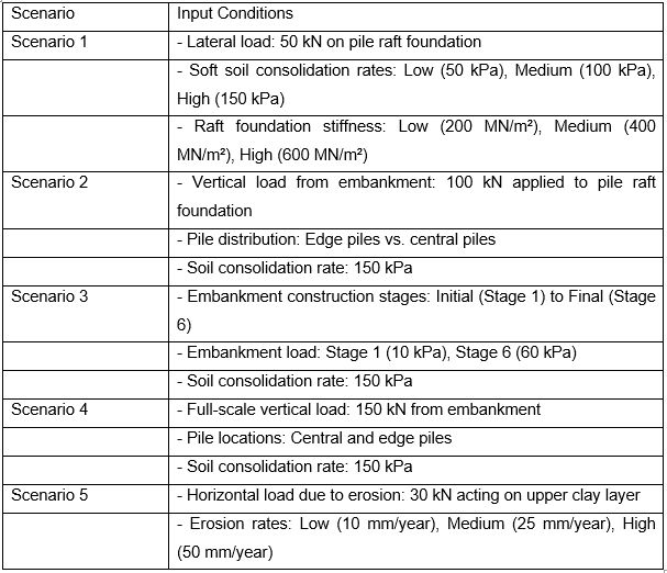
The aforementioned circuit can identify a defective underground wire if one is found. The location of the problem must be identified in order to be fixed. According to engineering assignment help, the law of Ohm is adhered to in this situation. The microcontroller 8051 is used in this. The ADC unit determines the length of the wire (in KM). The relays are controlled by a relay driver integrated circuit. Using it, the wire connections are tested. The data is read using an LCD device that is connected to a microcontroller. Using a certain method, several electrical or physical terms are calculated. This process is known as data acquisition (DAQ). DAQ uses variables such as sound, voltage, pressure, current, and temperature to calculate results. The schematic for a DAQ system employing an 8051 microcontroller was displayed on the preceding page. All the required tools are displayed in the diagram. A system should be equipped with all of the necessary components to increase its efficiency. It will be simple for the device to obtain data if the microcontroller is connected to the DAQ circuit. Any programme should include a human interface. To increase the effectiveness of the computer, people should interact with it properly. The other devices can only be linked using the user interface. In order to increase application efficiency, a network's necessary devices should all be connected.
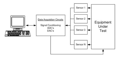
Figure 5:Data Acquisitions Block Diagram
The block diagram up top shows how the device is observed's data is being collected. The appliance is equipped with a variety of sensors. These sensors are connected to a computer through DAQ. DAQ places an order for the circuit upgrade. This improves the device's quality and function after being checked. The underground wire fault tracker's effectiveness may also be enhanced by it. When the DAQ circuit and alarm system are connected to the microcontroller, the alarm system may instantly identify the problem while also displaying the defect's location on the screen. It will boost the system's efficiency and dependability.
Figure 6: DAQ using 8051 microcontroller
The schematic for a DAQ system employing an 8051 microcontroller was displayed on the preceding page. All the required tools are displayed in the diagram. A system should be equipped with all of the necessary components to increase its efficiency. It will be simple for the device to obtain data if the microcontroller is connected to the DAQ circuit. Any programme should include a human interface. To increase the effectiveness of the computer, people should interact with it properly. The other devices can only be linked using the user interface. In order to increase application efficiency, a network's necessary devices should all be connected.
References


Download Samples PDF
Related Sample
- COMP1702 Big Data Assignment
- DFVP20001 Domestic and Family Violence Theories and Perspectives
- BEHL2009 Bachelor of Social Science Assignment
- MIS609 Data Management and Analytics Case Study
- BSBPMG430 Undertake Projectwork Assignment
- The Role of Technology in Architecture Assignment
- Technology and Engineering Management Assignment
- UMH207 Understanding Mental Health Assignment
- NURBN1015 Introduction to Evidence Based Practice and Research Assignment
- SOAD9206 Social Work Research in Practice Settings Report 1
- MEM602 Engineering Risk Management Assignment
- EDUC1001 Language and Learning in Your Discipline Assignment
- MIS610 Advanced Professional Practice
- MCR006 Financial Management Research Report 2
- MGT600 Management People and Teams Report 3B
- PRJ6001 Applied Project Assignment
- MITS4002 Object Oriented Software Development Assignment
- MGT602 Business Decision Analytics Assignment 2
- BIZ102 Understanding People and Organisations Assignment
- SRQ780 Strategic Construction Procurement Report 2

Assignment Services
-
Assignment Writing
-
Academic Writing Services
- HND Assignment Help
- SPSS Assignment Help
- College Assignment Help
- Writing Assignment for University
- Urgent Assignment Help
- Architecture Assignment Help
- Total Assignment Help
- All Assignment Help
- My Assignment Help
- Student Assignment Help
- Instant Assignment Help
- Cheap Assignment Help
- Global Assignment Help
- Write My Assignment
- Do My Assignment
- Solve My Assignment
- Make My Assignment
- Pay for Assignment Help
-
Management
- Management Assignment Help
- Business Management Assignment Help
- Financial Management Assignment Help
- Project Management Assignment Help
- Supply Chain Management Assignment Help
- Operations Management Assignment Help
- Risk Management Assignment Help
- Strategic Management Assignment Help
- Logistics Management Assignment Help
- Global Business Strategy Assignment Help
- Consumer Behavior Assignment Help
- MBA Assignment Help
- Portfolio Management Assignment Help
- Change Management Assignment Help
- Hospitality Management Assignment Help
- Healthcare Management Assignment Help
- Investment Management Assignment Help
- Market Analysis Assignment Help
- Corporate Strategy Assignment Help
- Conflict Management Assignment Help
- Marketing Management Assignment Help
- Strategic Marketing Assignment Help
- CRM Assignment Help
- Marketing Research Assignment Help
- Human Resource Assignment Help
- Business Assignment Help
- Business Development Assignment Help
- Business Statistics Assignment Help
- Business Ethics Assignment Help
- 4p of Marketing Assignment Help
- Pricing Strategy Assignment Help
- Nursing
-
Finance
- Finance Assignment Help
- Do My Finance Assignment For Me
- Financial Accounting Assignment Help
- Behavioral Finance Assignment Help
- Finance Planning Assignment Help
- Personal Finance Assignment Help
- Financial Services Assignment Help
- Forex Assignment Help
- Financial Statement Analysis Assignment Help
- Capital Budgeting Assignment Help
- Financial Reporting Assignment Help
- International Finance Assignment Help
- Business Finance Assignment Help
- Corporate Finance Assignment Help
-
Accounting
- Accounting Assignment Help
- Managerial Accounting Assignment Help
- Taxation Accounting Assignment Help
- Perdisco Assignment Help
- Solve My Accounting Paper
- Business Accounting Assignment Help
- Cost Accounting Assignment Help
- Taxation Assignment Help
- Activity Based Accounting Assignment Help
- Tax Accounting Assignment Help
- Financial Accounting Theory Assignment Help
-
Computer Science and IT
- Operating System Assignment Help
- Data mining Assignment Help
- Robotics Assignment Help
- Computer Network Assignment Help
- Database Assignment Help
- IT Management Assignment Help
- Network Topology Assignment Help
- Data Structure Assignment Help
- Business Intelligence Assignment Help
- Data Flow Diagram Assignment Help
- UML Diagram Assignment Help
- R Studio Assignment Help
-
Law
- Law Assignment Help
- Business Law Assignment Help
- Contract Law Assignment Help
- Tort Law Assignment Help
- Social Media Law Assignment Help
- Criminal Law Assignment Help
- Employment Law Assignment Help
- Taxation Law Assignment Help
- Commercial Law Assignment Help
- Constitutional Law Assignment Help
- Corporate Governance Law Assignment Help
- Environmental Law Assignment Help
- Criminology Assignment Help
- Company Law Assignment Help
- Human Rights Law Assignment Help
- Evidence Law Assignment Help
- Administrative Law Assignment Help
- Enterprise Law Assignment Help
- Migration Law Assignment Help
- Communication Law Assignment Help
- Law and Ethics Assignment Help
- Consumer Law Assignment Help
- Science
- Biology
- Engineering
-
Humanities
- Humanities Assignment Help
- Sociology Assignment Help
- Philosophy Assignment Help
- English Assignment Help
- Geography Assignment Help
- Agroecology Assignment Help
- Psychology Assignment Help
- Social Science Assignment Help
- Public Relations Assignment Help
- Political Science Assignment Help
- Mass Communication Assignment Help
- History Assignment Help
- Cookery Assignment Help
- Auditing
- Mathematics
-
Economics
- Economics Assignment Help
- Managerial Economics Assignment Help
- Econometrics Assignment Help
- Microeconomics Assignment Help
- Business Economics Assignment Help
- Marketing Plan Assignment Help
- Demand Supply Assignment Help
- Comparative Analysis Assignment Help
- Health Economics Assignment Help
- Macroeconomics Assignment Help
- Political Economics Assignment Help
- International Economics Assignments Help
-
Academic Writing Services
-
Essay Writing
- Essay Help
- Essay Writing Help
- Essay Help Online
- Online Custom Essay Help
- Descriptive Essay Help
- Help With MBA Essays
- Essay Writing Service
- Essay Writer For Australia
- Essay Outline Help
- illustration Essay Help
- Response Essay Writing Help
- Professional Essay Writers
- Custom Essay Help
- English Essay Writing Help
- Essay Homework Help
- Literature Essay Help
- Scholarship Essay Help
- Research Essay Help
- History Essay Help
- MBA Essay Help
- Plagiarism Free Essays
- Writing Essay Papers
- Write My Essay Help
- Need Help Writing Essay
- Help Writing Scholarship Essay
- Help Writing a Narrative Essay
- Best Essay Writing Service Canada
-
Dissertation
- Biology Dissertation Help
- Academic Dissertation Help
- Nursing Dissertation Help
- Dissertation Help Online
- MATLAB Dissertation Help
- Doctoral Dissertation Help
- Geography Dissertation Help
- Architecture Dissertation Help
- Statistics Dissertation Help
- Sociology Dissertation Help
- English Dissertation Help
- Law Dissertation Help
- Dissertation Proofreading Services
- Cheap Dissertation Help
- Dissertation Writing Help
- Marketing Dissertation Help
- Programming
-
Case Study
- Write Case Study For Me
- Business Law Case Study Help
- Civil Law Case Study Help
- Marketing Case Study Help
- Nursing Case Study Help
- Case Study Writing Services
- History Case Study help
- Amazon Case Study Help
- Apple Case Study Help
- Case Study Assignment Help
- ZARA Case Study Assignment Help
- IKEA Case Study Assignment Help
- Zappos Case Study Assignment Help
- Tesla Case Study Assignment Help
- Flipkart Case Study Assignment Help
- Contract Law Case Study Assignments Help
- Business Ethics Case Study Assignment Help
- Nike SWOT Analysis Case Study Assignment Help
- Coursework
- Thesis Writing
- CDR
- Research

.png)
~5.png)
.png)
~1.png)


.png)